Breadboard computer - Reset circuit
<Previous - This is part 2 of my series on building a breadboard computer. - Next>
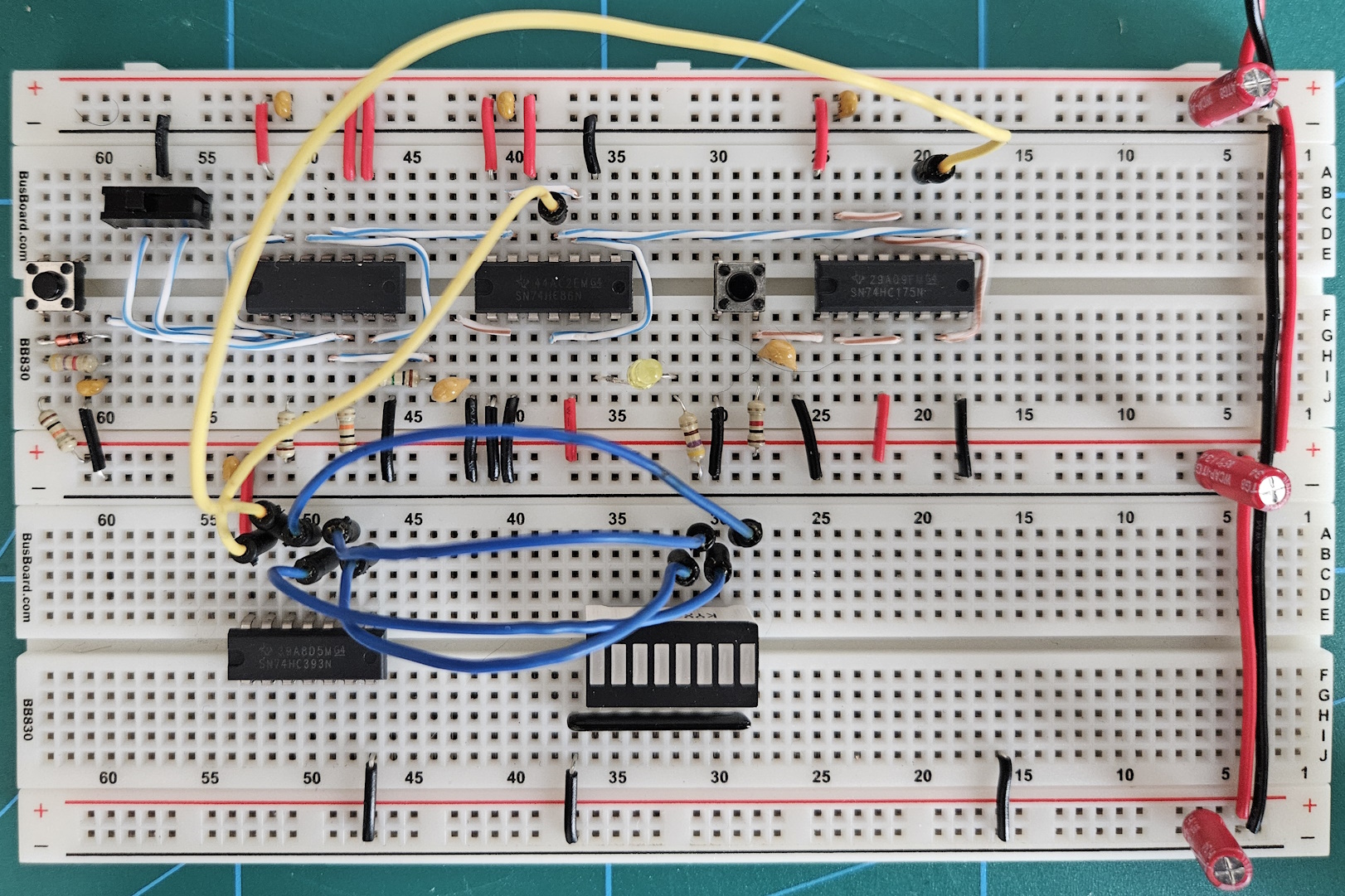
Reset synchronization
To be able to start from or reset to a known state I want to add a reset circuit to the computer. Since the computer will consist of many ICs of different kinds, the way to reset or clear them may differ. Some chips may have a reset/clear pint that will have to be pulled low (active low), while others may have to be pulled high (active high). In addition, some may be asynchronous which means the chip is reset immediately, while others are synchronous, which means they are reset only if the reset signal is active when the clock is pulsing. The same goes for releasing the reset signal.
To make sure every chip is reset simultaneously and synchronized with the clock, I’ll use a reset synchronizer circuit. The circuit is based on Fabian Schuki’s reset synchronizer from his Superscalar CPU build, his whole series is recommended after watching Ben Eater’s videos.
The circuit uses a chain of D flip-flops to hold the reset signal over several clock signals and synchronize the release of the reset signal with the clock. I have also added a capacitor to the circuit as Fabian did to make sure the computer starts up in reset mode on power on. The circuit can be seen below:
Building the circuit
The circuit was pretty easy to build, I used a 74HC175 quad D-type flip flop, a push button, and a 10k pull-up resistor and a 1uF capacitor.
Other changes
In addition to adding the synchronizer circuit I also changed the capacitor for the free-running clock circuit from 0.1 uF to 1 uF, changing the frequency from 20 Hz to 2 Hz. I also changed to color coded wires for different parts of the circuit instead to make building and troubleshooting easier. Finally, I moved to clock LED from the line between the NAND and XOR gates, and used a spare XOR to buffer it instead, as well as tying all unused inputs to either high or low. I tie all unused inputs so that the output is low, just to have a stanadardized way of doing it.
Next step
The next step of the build will be to come up with an overall design for the computer. Since I will have 256 bytes of RAM (8 address bits) instead of 16 bytes and use 1 byte instructions, I can’t follow the Ben Eater / SAP-1 design. I need an 8 bit address bus, and the RAM addressing and instruction decoding needs to be changed.
For example, should I connect the program counter directly to the memory bus, or copy the PC to the memory address register, like Ben does in his computer? I’m not well enough versed in computer architecture to have the answer to questions like these yet, so I have to do some research, thinking and design.